- Browse Repository
- University Libraries
- Kelvin Smith Library: Projects & Publications
- Art of STEM
- Quayle, Paul (x)
- Zhao, Hongping (x)
- Art of STEM 2015
Art of STEM 2015
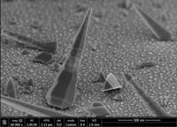
Show moreIndium nitride (InN) nanowires were synthesized on Si (100) substrate by chemical vapor deposition (CVD) method via a vapor-liquid-solid growth mechanism. The Si substrate was covered with 15 A Au film deposited via thermal evaporation. High purity Indium foil and ammonia were used as group III and group V sources respectively. The growth temperature and pressure were 580 C and 10 Torr respectively. The growth was conducted for 1.5 hr. The SEM image shows two different orientations of the InN nanowires; non polar m-plane with triangular cross section and polar c-plane with hexagonal cross section. The image was taken at the Swagelok Center for Surface Analysis of Materials (SCSAM) at CWRU.
Show less
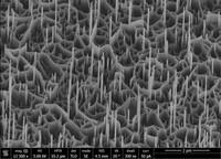
Show moreVertical ZnO 3D nanostructures were synthesized on Au covered c-plane GaN epilayer film on sapphire substrate by chemical vapor deposition method. The growth was conducted in a horizontal tube furnace with 1" diameter quartz tube. High purity ZnO powder and oxygen were used as the precursors. The growth was carried out for 1 hr at 900 C. The growth direction was polar. The image shows the 20 degree tilted view of the nanostructures. The image was taken at the Swagelok Center for Surface Material Analysis (SCSAM) at CWRU.
Show less
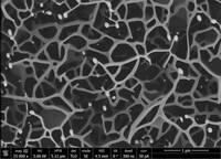
Show moreZnO 3D nanostructures composed of an array of 1D nanowires and 2D nanowalls were synthesized by chemical vapor deposition (CVD) method on c-plane GaN epilayer covered sapphire substrate. The nanowire growth followed vapor-liquid-solid (VLS) growth mechanism and the nanowall growth followed vapor-solid (VS) growth mechanism. The substrate was covered by 5 nm Au film deposited by thermal evaporation. High purity ZnO powder and oxygen were used as the source materials and argon as carrier gas. The growth temperature was 900 C. The nanostructures grew vertically along polar c-plane orientation. The field emission scanning electron microscopy (FESEM) show the top view of the 3D nanostructures. The image was taken at Swagelok Center for Surface Analysis of Materials (SCSAM) at CWRU.
Show less